At present, the best-selling product in the semiconductor industry is undoubtedly DRAM. With the boost of the storage super cycle, global DRAM manufacturers have experienced successive waves of chip manufacturing. Friends familiar with semiconductor process technology know that the production of storage chips also relies on three major processes: wafer preparation, front-end wafer manufacturing, and back-end packaging and testing. The following mainly introduces the part related to lasers in the front-end wafer manufacturing - edge bead removal (EBR).
I. What is the Edge Bead Removal
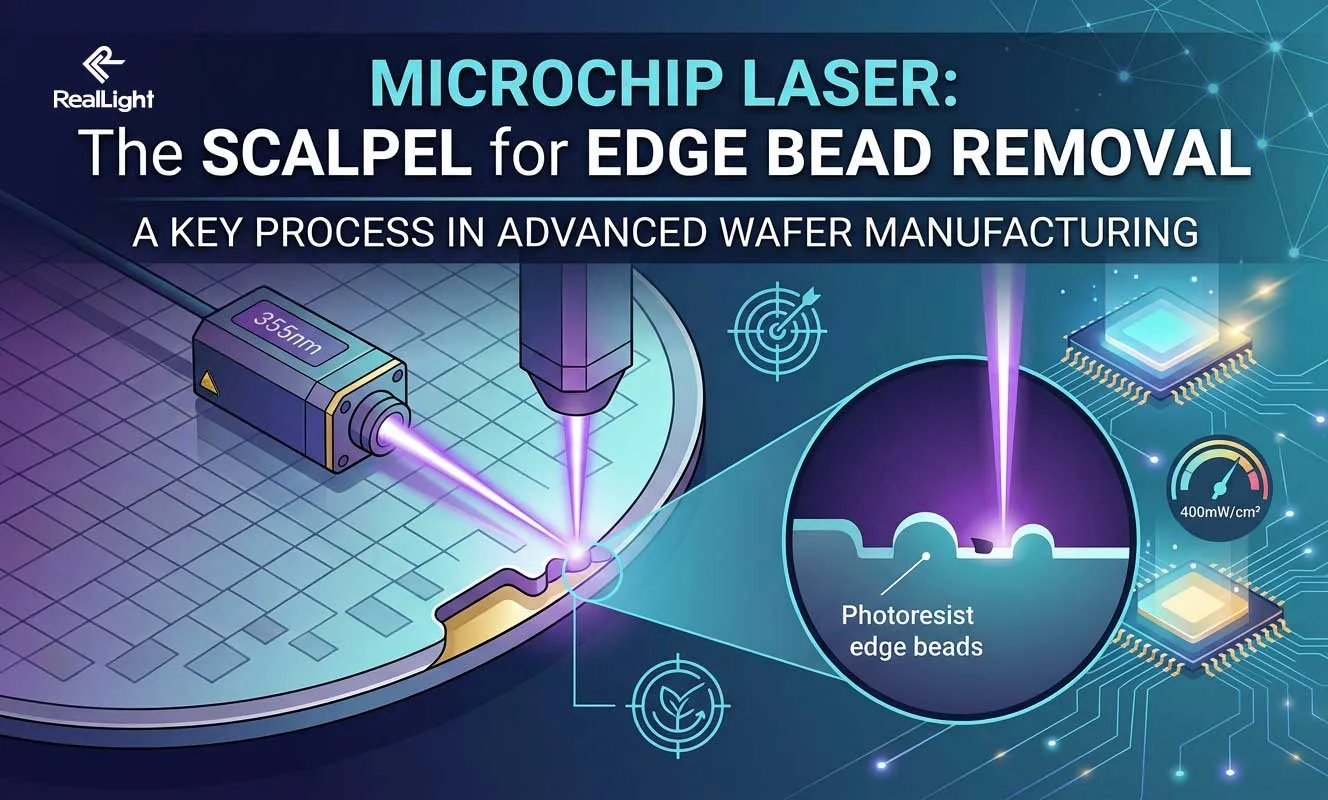
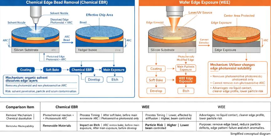
It is well known that before performing lithography on a chip, a layer of photoresist must be applied. After going through the two processes of pre-treatment and spin-coating, the excess photoresist is often pushed to the edge of the wafer by centrifugal force. Some of it is thrown off, and some remains. Due to the relatively fast airflow speed at the edge of the wafer, the remaining photoresist quickly cures. From a cross-sectional view, the entire chip looks like two small hills, and this part is called "edge beads". The equipment uses a special method to wash away these excess thick photoresist, which is called " edge bead removal". This step is crucial because the remaining "edge beads" will become a source of particle contamination in the subsequent processes. Therefore, the EBR treatment must be carried out.
II. Industry-Standard Repair Solutions
Currently, the two mainstream EBR methods in the industry are chemical EBR and optical EBR. Chemical EBR uses a jet of solvent to dissolve the edge glue, and then it is centrifuged to be ejected. Optical EBR is also known as wafer edge exposure (WEE). Its core principle is to use ultraviolet laser to irradiate the edge, and simultaneously dissolve during the development process. The significant advantages of intersecting chemical EBR and optical EBR are that there is no risk of chemical solvent splashing, and the boundary contour is more regular. What's more convenient is that the WEE module is usually highly integrated within the coating and developing machine, and does not occupy additional space. Under such application conditions, the micro-laser has a significant size advantage.
III. Key Process Parameters of the System
It seems like just a simple exposure, but in mass production, this process requires extremely strict control over both precision and energy. First, the gap positioning accuracy must be controlled within the range of ±0.2° to prevent misalignment of the exposed area. The edge exposure position accuracy needs to be controlled within the range of ±0.3mm to ensure that only the edge waste resin is removed and the central effective area is protected. Finally, the exposure usually requires a power density greater than 400mW/cm²; otherwise, the power will not be sufficient to leave a fatal contamination source for the subsequent production process due to the chemical reaction of the photoresist. Microchip lasers often have both high peak power and small spot size, which have unique advantages in WEE applications. In modern advanced support production lines, WEE is highly favored not only because it completely avoids chemical solvent splashing, but also because with increasingly advanced chip manufacturing processes, edge accuracy requirements will become higher and chemical EBR will be difficult to further improve.
IV. Adaptability of Microchip Lasers
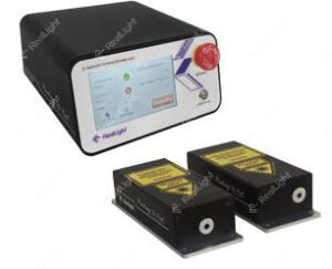
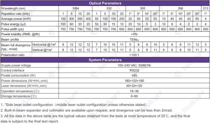
A microchip laser is a type of laser that can achieve excellent beam quality and peak power easily. It does not have very high laser power or laser energy, but its short cavity length feature enables a pulse width of sub-nanoseconds, with an exceptionally high peak power, which particularly compensates for the edge defects caused by thermal accumulation in photomask materials. Just with this feature, microchip lasers can demonstrate unique advantages in fine processing. The mainstream i-line lithography process generally uses a laser with a wavelength of 355nm. This wavelength laser has a high commercialization level, relatively mature process and technology, and good stability, which is in line with the characteristics of microchip lasers. For applications like WEE, microchip lasers truly achieve compact and efficient design. The MCC series RealSubns® microchip lasers launched by RealLight for this industry have a high single-pulse energy, clean pulses without tails, excellent beam quality, and are precisely the choice with high cost-effectiveness for WEE applications.
V. Summary and Outlook
This article mainly introduces the optical repair method in the edge bead removal (EBR) and the corresponding high-performance laser. For integrated devices that are sensitive to volume and cost but have low power requirements, the microchip laser is very suitable, and its high adaptability perfectly meets the WEE application. However, the pulse jitter characteristic brought by the passive Q-switching of this laser may also limit the design of the solution. Moreover, its pulse width is still far less than the ultra-fast laser, and it cannot achieve the ultimate effect of true "cold processing".
The future of WEE technology will require adaptation to more advanced processes, larger wafer sizes, and higher yield requirements. It will evolve from a simple cleaning tool to a precise control link in semiconductor manufacturing. With the advancement of the manufacturing processes of various semiconductor companies, RealLight independently developed ultraviolet pulsed laser will provide assistance for the precise control in semiconductor manufacturing.
Disclaimer: Some content in this article is sourced from the internet for the purpose of technical research and exchange. It is intended for reference and learning only. If there are any inaccuracies or academic discrepancies, please feel free to provide feedback. For copyright concerns, please contact us, and we will promptly verify and remove any infringing content.
References
MCC Series 750ps Microchip Laser