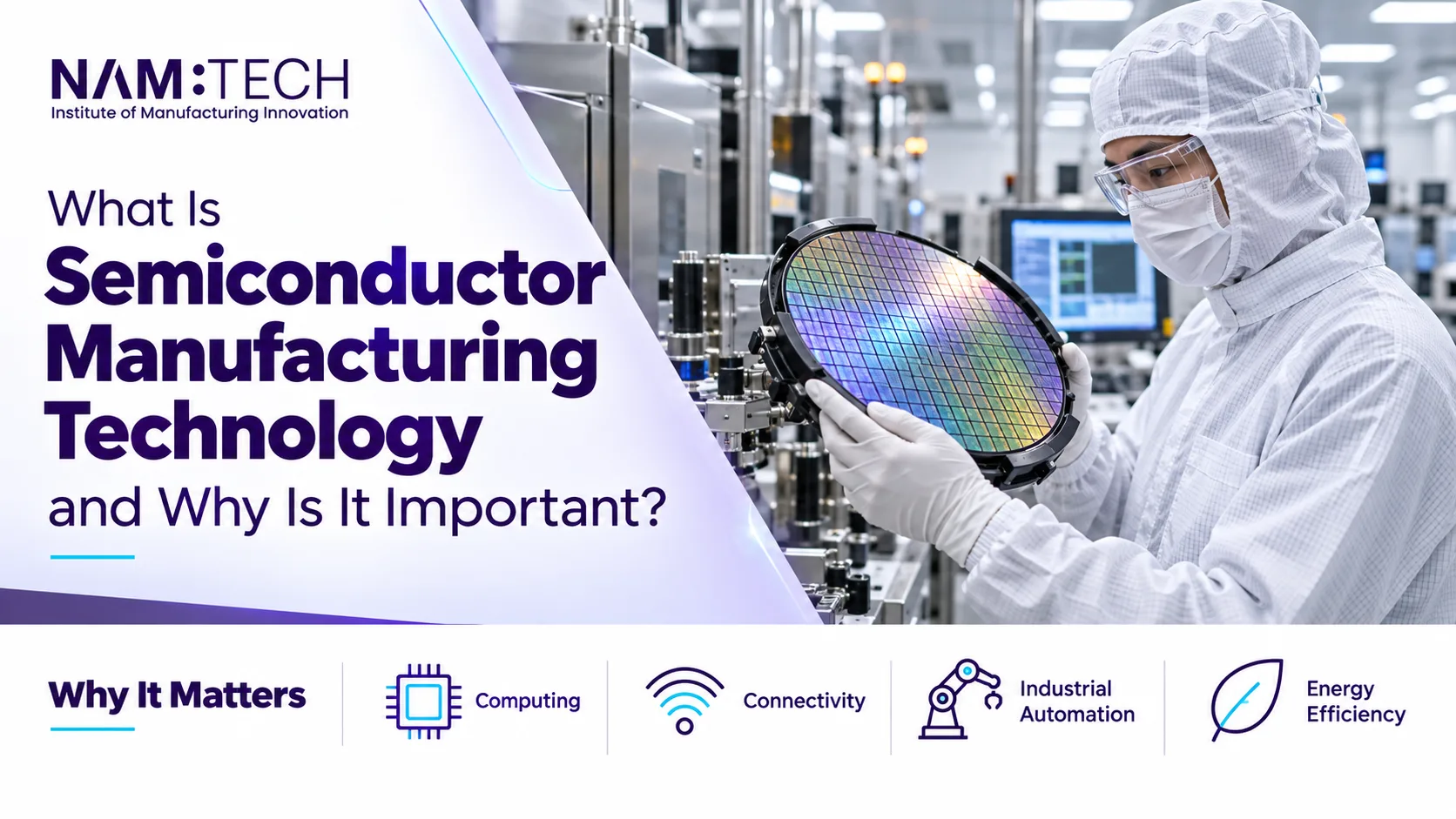
Every phone, car and hospital scanner relies on chips, yet most people never think about where they come from. Chips begin as a polished disc of silicon called a wafer, and turning that disc into working devices takes thousands of steps over more than three months. A single speck of dust can ruin the circuits beneath it. That mix of extreme precision and huge scale is what semiconductor manufacturing technology covers.
What happens inside a chip factory?
The factory is called a fab, short for fabrication plant. Inside, wafers move through a loop of the same few operations, repeated layer after layer. Deposition lays down a thin film of metal or insulator. Photoresist, a light-sensitive coating, goes on top. Lithography shines light through a stencil called a mask to print a pattern into that coating. Etching then removes material wherever the pattern says so, using chemical baths or gases. Doping adds tiny amounts of other elements to change how the silicon conducts electricity. Repeat that loop many times, test the wafer, cut it into individual chips and package them.
Why is it so hard to get right?
Because the margin for error is tiny. Circuit features are measured in nanometres, a billionth of a metre, so a speck of dust can wreck a layer. That’s why fabs run inside cleanrooms, and why designers go to great lengths to keep out vibration.
Then there’s yield, the share of chips on a wafer that work. Every defect lowers it, and a low yield turns an expensive process into a wasteful one. Much of process engineering is tracking down why yield dipped.
Money adds pressure. A modern fab can cost between five and 20 billion dollars, and most of that goes on equipment, not the building. A single extreme ultraviolet lithography machine can cost as much as 120 million euros. With that much capital tied up, an idle tool is expensive, and a stoppage from an electricity failure or missing process gas can take weeks or longer to recover from.
Why does it matter so much?
Chips sit inside most modern electronics, from phones and cars to medical equipment and the servers behind AI. Global chip sales reached about $796 billion in 2025, up roughly 26% on 2024, and industry forecasts put 2026 close to $1 trillion. Yet a clever chip design is only a drawing until someone can make it reliably, at volume.
Governments have noticed too. The US and the EU have each committed tens of billions to chipmaking and related training.
Are there enough jobs, or is it hype?
The shortage is documented, though most figures come from the US. A 2023 industry study projected that the American semiconductor workforce would grow from around 345,000 to about 460,000 by 2030, with roughly 67,000 of those jobs at risk of going unfilled. By its estimate, the gap splits roughly 39% technicians, 41% engineers and 20% computer scientists. Germany and Taiwan have reported similar shortages of skilled workers. These are projections, not promises, and local demand differs.
Which jobs exist inside a fab?
Technicians run and repair the tools, and they’re the people who keep wafers moving. Process engineers own a single step, such as etching, and tune it until it’s stable. Equipment engineers keep the machines healthy. Yield engineers hunt defects across the whole flow. Device engineers shape how the transistors themselves behave. Manufacturing managers tie it all to schedules and cost.
Say yield dips on a Tuesday. The yield engineer pulls the data, the process engineer checks the etch recipe and a technician inspects the tool. One problem, three angles.
Do you need a master’s degree to work in a fab?
No. Technician roles usually start with a technical diploma or two-year degree, and technicians make up about two-fifths of that projected gap.
A Master Program in Semiconductor Manufacturing Technology is aimed at people who want to design and improve the process, not just run it. Applicants usually hold a bachelor’s degree in engineering, chemistry, materials science, physics or a close subject.
What does a master’s programme teach?
Content varies by university, but a Master Program in Semiconductor Manufacturing Technology generally covers the core process steps in depth, then adds the parts that decide whether a fab makes money. Typical topics include clean room design and operation, process integration (how the steps fit together into a full chip), yield management and defect reduction, and process control. Some programmes use case studies on real yield problems, and others have students design a complete fabrication flow in a small group.
How do you pick a programme worth the fees?
Start with the facilities. A Master Program in Semiconductor Manufacturing Technology with no cleanroom time, and no access to real process tools or credible simulation, leaves a gap that employers will notice. Ask which equipment students use, whether fabs or equipment makers sponsor projects, and where graduates work now. Look for named outcomes such as process engineer or yield engineer, not a vague promise of a career in tech.
Which skills help most?
The subject mixes physics, chemistry, materials science and electronics, so a solid grounding in at least one helps. Statistics matters more than most students expect, since process control and yield work depend on reading data and spotting drift (slow changes in a process). Comfort with scripting, such as Python, is useful for the same reason. Fab work follows written procedures to the letter, because a skipped step can scrap a whole batch of wafers, and the patience to follow them counts as much as brilliance.
Where can the degree lead?
Graduates of a Master Program in Semiconductor Manufacturing Technology commonly aim for process, equipment, device, or yield engineering roles at foundries (factories that make chips designed by other firms), chipmakers and tool suppliers, with the option of moving into manufacturing management later. The same skills carry over to related industries that also work in cleanrooms or with thin films, such as display and solar manufacturing.
What are the downsides?
Fabs usually run around the clock, so shift work is common for technicians and sometimes for engineers. Working in a cleanroom means wearing protective clothing for most of the shift. The industry is also cyclical: memory chip sales were still recovering from a 2023 downturn during 2025, and hiring can follow such swings. Employers cluster in a few regions, so moving for work is a real possibility.
Where does that leave a student?
Semiconductor manufacturing is a craft built on repetition, precision and patience, and its importance comes from a simple fact: most digital products depend on someone able to make the chips. For a student, the real choice is how deep you want to go. A technical course gets you onto the floor sooner. A Master Program in Semiconductor Manufacturing Technology takes longer but opens the engineering side, where decisions about process and yield get made. Neither route is the wrong one. The question worth sitting with is simple: when a process goes wrong, do you want to be the one who finds out why?